
The demand for ever more powerful and compact electronic devices is constantly growing. However, in times of rising raw material and energy prices, developers, engineers and companies are faced with the challenge of finding the right balance between quality and cost-effectiveness when developing high-performance components. This also applies to printed circuit boards as the backbone of electronic circuits.
But where are the starting points for acting as efficiently as possible in view of the cost explosion on the procurement markets? Printed circuit boards actually offer numerous opportunities to realize potential cost savings through technical adjustments. Biggest Influencing factor is the base material with an average share of 35 % in production costs. It is important to choose the right material, make maximum use of it and optimize the layer structure.
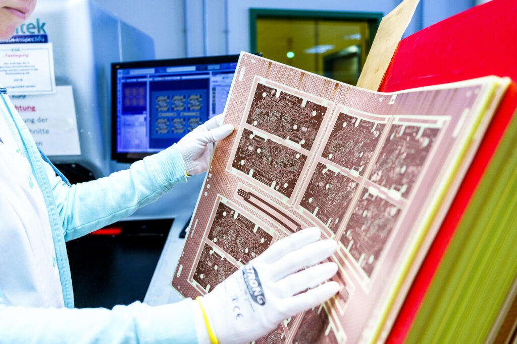
Choosing the right material
When selecting the right material for printed circuit boards, several factors play a decisive role, influencing not only the technical performance but also the costs. In principle, the Base material type should always be selected according to the operating temperature and thermo-mechanical stress. It is important to consider the specific requirements of the application in order to ensure optimum performance and service life of the PCB.
Standardization is also key. For this reason, the focus should be on Standard superstructures where this is technically possible. These not only offer proven structures, but also facilitate availability and cost-effectiveness. It is also advisable to use standard values when determining laminate thicknesses.
Further recommendations from the KSG experts:
- Concentrate on dual-ply structures for prepregs.
- Make the layout as large as possible, because tight line space requirements are not only a cost factor in terms of material, but also due to the required yield reduction.
In view of the copper price trend, use 18 and 35 µm base copper wherever possible.
Making maximum use of the material
True to the motto "Refined scrap costs money", material utilization has a direct impact on all process costs. Early coordination with the manufacturer is therefore crucial in order to ensure maximum utilization of the material for printed circuit boards. It is advisable to discuss the utilization design intensively as early as the planning phase. The focus here should be on individual part specifications and minimum requirements in order to create room for efficiency increases. With the help of our Technical supportThe ideal use of the materials in your production-ready PCB can be simulated. This simulation not only enables precise planning, but also the optimization of cost structures.
Further recommendations from the KSG experts:
- Consider scoring instead of milling for contour processing. Cost savings of up to 12 % are possible here.
- Use the design-to-cost recommendations in the Digital Design Compass of the KSG Group.

The Digital Design Compass provides you with crucial PCB information and design rules for all KSG technologies.
Optimize the layer structure
Cost reduction potential can also be tapped into when designing the layer structure by taking the following factors into account:
- Reduce the number of layers and thus save material costs and an entire IL production run (6-12 operations).
- Avoid multiple pressing, as this means significantly higher production costs.
- Avoid buried vias and make all connections from the outer layers if possible.
How do you feel about this topic? Find out in Part 2 and Part 3 of our series of articles where further savings potential can be exploited on the way to cost-efficient PCBs.