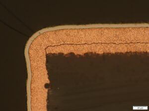
The Soldering surface electroless nickel/gold (chem. NiAu) is also known as ENIG (Electroless Nickel Immersion Gold). In a wet-chemical process, a 3 to 6 µm thin layer of nickel (phosphorus-doped) is first deposited on the copper surfaces of the component connections. The nickel layer forms a barrier for the 0.05 to 0.12 µm thin gold layer, which is then also applied chemically. During the soldering process, the nickel/gold layer wets itself quickly and evenly with the solder. A sequence of nickel/tin intermetallic phases with different compositions forms between the tin of the solder alloy and the nickel of the solder surface. The gold is completely dissolved during the soldering process. Ideally, after the solder has solidified, there is a uniform metallic zone a few micrometers thick that adheres firmly to the substrate and enables reliable SMD solder connections.
Planar surface and 12-month shelf life
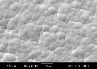
In addition to a planar soldering surface, NiAu also offers a long shelf life. With proper Storage the PCB manufacturer provides a 12-month solderability warranty. The wetting of the solder pads is evaluated according to the J-STD-003 standard. The resulting nickel/tin alloy is more brittle than a copper/tin connection. The soldering surface is therefore not recommended for electronic assemblies that are exposed to strong bending or vibrations. Chemically NiAu is RoHS-compliant and described in IPC-4552. The layer thicknesses are measured non-destructively with an X-ray fluorescence test or in a destructive test with a microsection analysis. However, only the nickel layer is visible in the micrograph. The gold layer is too thin to be detected and measured in the micrograph.
The nickel/gold surface is also suitable for switching contacts and wire bonding. ENIG is predestined for aluminum wire bonding in accordance with MIL-STD 883. In our opinion, the gold layer is too thin for gold wire bonding. However, we have customers who have validated the bonding process for themselves and for whose applications the gold wire base works. Chemically NiAu is only suitable for press-fit technology to a limited extent because nickel is brittle and hard. However, our customers have also validated the process for themselves.
The combination with electroplated nickel/gold on the connector contacts at the edge of the PCB is possible. The electroplated gold surface for PCB connectors (hard gold or connector gold) is significantly thicker and more robust than with ENIG.
The most commonly used soldering surface
Chemically NiAu is the most commonly used soldering surface in Europe. An estimated 50 % of all PCBs manufactured in Europe have this finish, and the trend is rising (source: ZVEI). At KSG, ENIG is also by far the most commonly used PCB finish by customers. We estimate that with the increase in fine and ultra-fine conductor technologies, the production share of this surface will continue to rise.