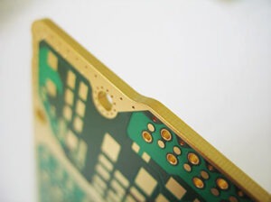
Thick copper PCBs, manufactured using pure etching technology, are the first choice for high currents
and are characterized by structures with copper thicknesses from 105 to 400 µm.

HDI stands for "High Density Interconnect". These are multilayer PCBs with four or more layers that are built up sequentially ("Sequential Build Up" or SBU) in several press cycles.
This achieves higher packing densities and meets the requirements of state-of-the-art component development. This opens up completely new possibilities for your PCB layout in order to meet the ever-increasing miniaturization, which demands ever more complex circuits and components with extremely high pin counts.
Thanks to state-of-the-art production technology, layouts from a line/space of 75 µm are possible. The filling technologies of drill holes (e.g. microvia copper filling, plugging or resin filling) play a decisive role in the selection of an optimal rewiring strategy.

| Materials | FR4 (thermostable) |
| Number of layers | 2-8 |
| PCB thickness | 0.5 mm - 3.2 mm |
| End copper outer layers | 50, 70, 105, 175, 210 µm |
| End copper inner layers | 70, 105, 210, 400 µm |
| Ladder structures | Depending on the final copper according to the design compass |
| Smallest drill diameter | min. ⅔ of the total copper thickness |
| Aspect Ratio | ≤ 1:6 |
| Surfaces | See general technical specifications, no HAL |
The specified values represent the maximum power spectrum and may be limited in certain combinations.
Solder resist masks
Additional prints
Edge metallization
In order to improve the EMC protection of a circuit board, to create an electrical contact to the housing of the assembly or to meet increased cleanliness requirements, the front sides of the circuit board contour can be metallized.

Milled vias
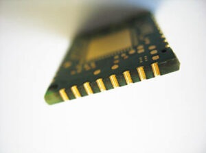
It is possible to produce application-specific components with so-called milled through-holes. The resulting circuit boards can be soldered onto another circuit board as components (interposer) due to their front-side contacting option.

Contour processing
Contour production: milling and scoring

The smart platform for fast and reliable PCB development.
We have bundled all the parameters for you in our Design Compass.
Take advantage of the direct line to the experienced PCB experts in our technical support team. We are happy to support you in every phase of your project.

Talk to us in the early development phases of your project and contact our team of experts. Together we will find the solution that will make your product even better.

With a workshop at our premises or at your site, we give you the opportunity to discuss the key technical aspects and features of your project in detail.

From design and layout checks to various calculations and thermal analyses - the experienced, competent Technical Support team will be happy to help you.