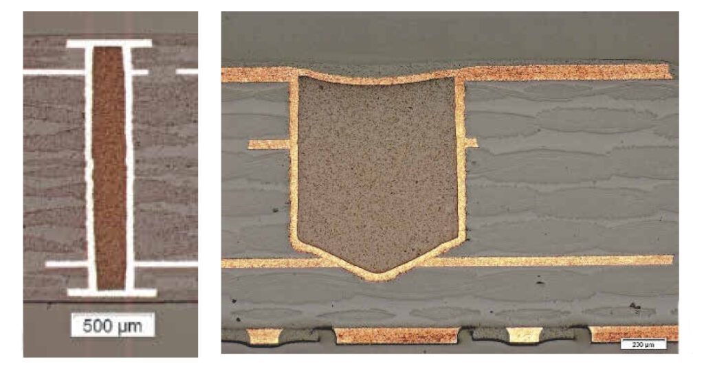
Plugging, Holefilling, Microvia Copper Filling or Via hole plugging refers to the filling of metallized through-holes or metallized blind holes on the outer layers of the PCB. This achieves a planar surface topography even with highly complex circuit carriers, which can significantly increase process safety and reliability in the assembly process, no solder run-off, no air inclusions.
The results are Filled-and-capped vias. Components can be placed directly via these vias and the integration density can be increased. The advantages are a considerable gain in space with SBU build-ups (SBU: sequential build up) and fewer restrictions in the layout design of complex circuits.
The metallized holes are filled with a special plugging paste and then metallized. There are various technological options for inserting the paste into the hole, each with their own specific advantages and disadvantages:
- Roller coating process
- Screen printing process
- Stencil printing process
- Vertical vacuum filling
KSG has opted for full-surface, vertical vacuum filling due to the wide range of applications. In addition to through-holes, this process also makes it possible to fill mechanically drilled or laser-drilled blind holes quickly, reliably and reproducibly and is therefore available for many applications. Further advantages over conventional screen printing processes are the air bubble-free filling of the holes, a high degree of flexibility, lower paste consumption and the filling of holes with a larger aspect ratio.