Search
Close this search box.

Iceberg® printed circuit boards

Iceberg®-PCBs are characterized by structures with mixed copper thicknesses from 105 to 400 µm in outer layers - with a uniform surface topography. High currents and fine conductors can be efficiently combined in a multilayer with optional inner layers.

Your advantages

We are happy to support you in every phase of the realization of your  Iceberg® printed circuit board.
Contact our team of experts here.

Iceberg® printed circuit boards

Increasingly powerful components require more and more power and emit more and more heat loss. To ensure the reliability of the circuit in the long term, the printed circuit board must also meet these requirements. Thick copper/iceberg®-PCBs are characterized by structures with mixed copper thicknesses of 105 to 400 µm in outer layers - with a uniform surface topography. High currents and fine conductors can therefore be efficiently combined in a multilayer together with additional optional inner layers.

These circuit boards are used for large (high) current outputs and for cooling for good thermal management. This is because the copper favors heat dissipation. They are usually designed as multilayer boards. 

Whether thermal management or current carrying capacity, thick copper and know-how are required here. KSG can provide you with both to suit your project.

Technology comparison table for high-current HSMtec® printed circuit boards
MaterialsFR4 (thermostable)
Number of layers2 – 8
PCB thickness1.5 mm - 3.2 mm
End copper outer layers105 and 400 µm
End copper inner layers18, 35, 70, 105, 210 µm
Ladder structuresDepending on the end copper according to Design Compass
Smallest drill diametermin. ⅔ of the total copper thickness
Aspect Ratio≤ 1:6
Surfaces
  • See general technical specifications
  • no HAL

The specified values represent the maximum power spectrum and may be limited in certain combinations.

  • Electroless nickel/gold
  • Immersion tin
  • Electroplated nickel/gold
  • OSP
  • More on request

Solder resist masks

  • Photosensitive coating systems, thermal final curing
  • Colors: green, red, blue, black glossy, black matt, white, yellow
  • Non-photosensitive coating systems, purely thermal curing: white, black


Additional prints 

  • Labeling/equipment
  • Hole filler/through-hole filler
  • Peelable lacquer
  • Heatsink
  • Carbon


Edge metallization 

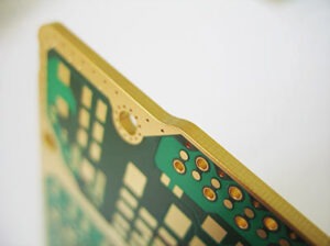
In order to improve the EMC protection of a circuit board, to create an electrical contact to the housing of the assembly or to meet increased cleanliness requirements, the front sides of the circuit board contour can be metallized.

Milled vias 

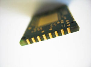
It is possible to produce application-specific components with so-called milled through-holes. The resulting circuit boards can be soldered onto another circuit board as components (interposer) due to their front-side contacting option.

HDI printed circuit board with milled through-hole plating

Contour processing

Contour production: milling and scoring

Microvias (lasered) on outer layers

Microvia's superstructure variant on outer layer

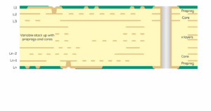
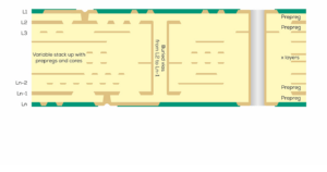
Microvias (lasered) in combination with plated-through laminates (mechanically drilled)

Microvia's construction variant with uch-contacted laminates (lasered)

Microvias (lasered) in combination with buried vias (mechanically drilled)

Microvias assembly variant with buried vias (mechanically drilled)

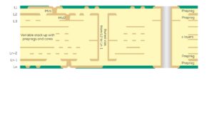
Staggered microvias (lasered) in combination with buried vias (mechanically drilled) - from L2 to Ln-1

Staggered microvias (lasered) in combination with buried vias (mechanically drilled)

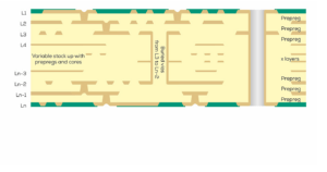
Staggered microvias (lasered) in combination with buried vias (mechanically drilled) - from L3 to Ln-2

Staggered microvias (lasered) with buried vias (mechanically drilled) from L3 to Ln-2

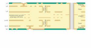
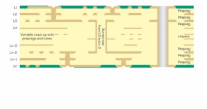
Stacked microvias (lasered) with microvia copper filling in combination with buried vias (mechanically drilled)

Staggered microvias (lasered) with buried vias (mechanically drilled) from L2 to Ln-1

Double Core

Layer structure of an HDI multilayer with 8 layers (4x4)

  • Use filled thermostable base materials with low Z-axis expansion 
  • Calculate resin filling level (material-dependent pre-calculation using the layer build-up program at KSG) 
  • Use sufficiently resin-rich prepregs 
  • Avoid "stacked" copper surfaces and copper-free areas 
  • Evenly distribute copper surfaces and copper-free areas 
  • Fill large copper-free areas with copper 
  • Create sufficiently large residual rings
Preview Digital Design Compass Banner

Digital Design Compass

The smart platform for fast and reliable PCB development.

We have bundled all the parameters for you in our Design Compass.

Technical support

Make a request

Talk to us in the early development phases of your project and contact our team of experts. Together we will find the solution that will make your product even better.

TS Meeting

Workshop & online consultation

With a workshop at our premises or at your site, we give you the opportunity to discuss the key technical aspects and features of your project in detail.

Mr. Hackel, Technical Support

Co-Engineering & Support

From design and layout checks to various calculations and thermal analyses - the experienced, competent Technical Support team will be happy to help you.

Iceberg®-PCBs are partial thick copper PCBs with mixed copper thicknesses of 105 and 400 µm on the same level in the outer layers. Around two thirds of the thick copper is embedded in the base material. The "sinking" of the thick copper structures in the base material enables a uniform surface topography despite different copper thicknesses on the same layer. This means that the conductor flanks can be reliably covered with solder resist in just one casting process.

Due to its planar surface, which simplifies loading, the Iceberg®-principle for thick copper PCBs with a copper cladding >250 µm on the outer layers. Iceberg®structures are also suitable as heat sinks for power components and can be combined with plated-through holes (vias) to optimize thermal management. In a wiring level, there are areas with 70 to 105 µm copper for the control electronics and areas with 400 µm copper for the load. This makes it possible to combine large cross-sections for high currents and fine conductors in a multilayer with optional inner layers. On the inner layers, the Iceberg®-principle can also be combined with thick copper.

The advantages of the Iceberg®-technology are:

Recommendations for the layer structure

Iceberg circuit board principle
Principle of iceberg PCB technology: thick copper structures are embedded in the base material
en_USEnglish