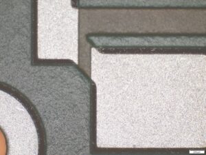
For the Soldering surface chemical tin (chem. Sn) or ISn (immersion tin), a 0.8 to 1.4 µm thin tin layer is deposited on the copper surfaces in a wet chemical process. According to IPC-4554, this is ≥ 0.6 µm pure tin (usable tin). The tin layer forms a planar soldering surface and thus provides the prerequisite for very good solderability of the finepitch components. After deposition, an intermetallic connection zone (IMC) is created. With proper Storage the PCB manufacturer provides a 9-month solderability warranty. The wetting of solder pads is assessed according to J-STD-003. A lack of wetting during the soldering process can be easily detected visually and by X-ray.

Immersion tin is RoHS-compliant and is suitable for press-fit technology and special micro press-fit technology. However, this surface is unsuitable for any wire bonding processes. As a soldering surface, immersion tin can be combined with an electroplated nickel/gold surface for plug contacts. Immersion tin and OSP (Organic Solderability Preservative) are the only soldering surfaces that can be refreshed on an industrial scale in the event of overlapping or poor solderability.
Addition of silver prevents whisker formation
Whisker formation is a possible defect in pure tin. Whiskers are very fine single crystals with a diameter of around 0.3 to around 10 µm and a length of up to several millimeters, which form on the tin surface and can cause short circuits. The formation of tin whiskers can be reliably prevented by the addition of silver. So-called organic metals are also used as an alternative to silver. Immersion tin is also described as a self-limiting process because the deposition process of the tin ions is only active for as long as free copper surface is available. The advantages are short process times at around 70 °C, which only minimally stress the base material and the solder resist of the printed circuit board.
Tin diffusion in copper can be accelerated by the effect of temperature. The chemical tin surface is therefore sensitive to thermal processes, e.g. the curing of lacquers that are applied after the soldering surface or drying processes when processing rigid-flex printed circuit boards. For this reason, there are special drying recommendations and limited solderability. The layer thicknesses of the tin are determined non-destructively using X-ray fluorescence analysis. The assumed density factor for the X-ray fluorescence measurement is 7.3 g/cm³. A pure tin layer thickness measurement, on the other hand, is only possible with a destructive coulometric measurement. In a direct comparison of process costs, immersion tin is significantly cheaper than electroless nickel/gold. Tin is the third most commonly used soldering surface for KSG customers.

