Rigid-flex PCBs are the ideal solution when several rigid PCBs need to be electrically connected in different installation positions and orientations.

Rigid-flex PCBs are the ideal solution when several rigid PCBs need to be electrically connected in different installation positions and orientations. With our rigid-flex PCBs, we offer solutions for every static bending load with the highest quality, cost-effectiveness and flexibility.
As soon as multiple bends are required. Rigid-flex PCBs are the ideal solution when several rigid PCBs need to be electrically connected in different installation positions and orientations. Rigid-flex PCB technology is particularly versatile in terms of layout options and geometries. And it is an indispensable component of modern connection technology:
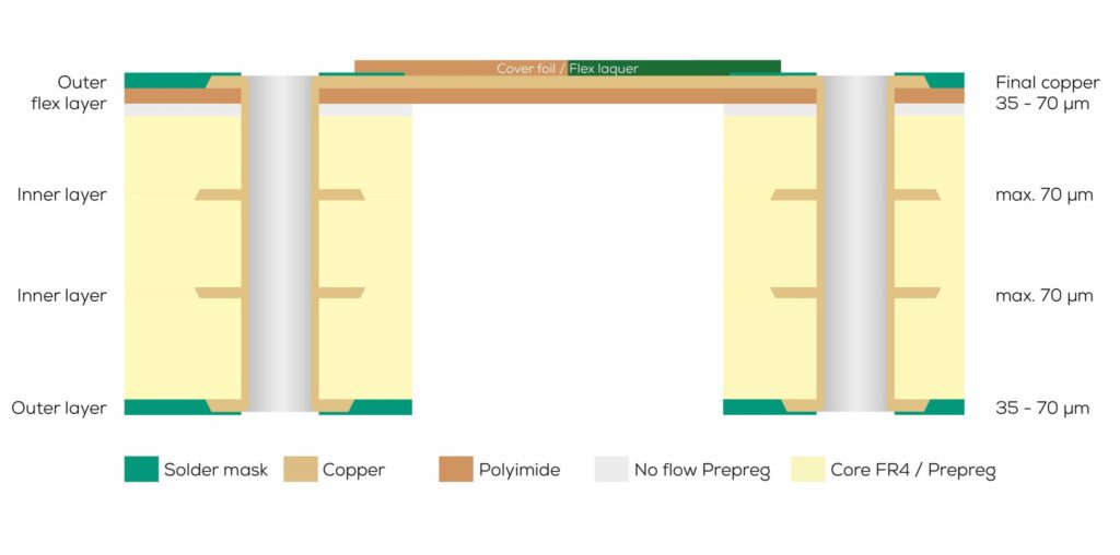
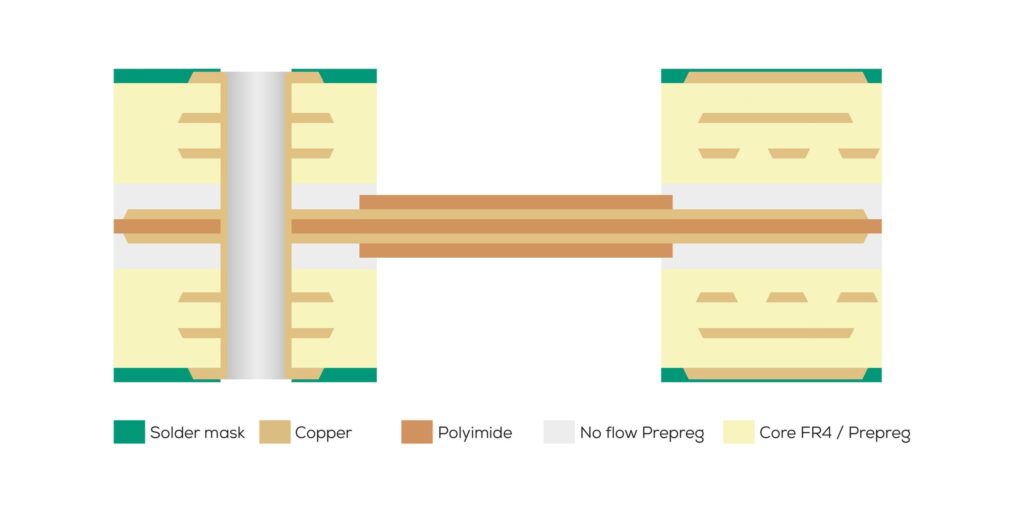
The manufacturing process is characterized by the pressing of two different types of material. First, the FR4 cores are produced in the same way as a multilayer. At the same time, the single or double-layer flex circuit is produced on polyimide. These semi-finished products are then pressed into a rigid-flexible composite using a separate pressing process, with so-called low-flow or no-flow prepregs serving as the composite material.
These composite layers are mechanically structured before the pressing process. This means that the subsequent flexible areas are milled out to prevent the FR4 cores from bonding to the polyimide material. This is followed by further processing in standard processes. Finally, during contour processing, the transitions from the rigid to the flexible areas are deep-milled with a groove, thus removing the unglued rigid material over the flexible areas.

| Materials | Polyimide / FR4 |
| Number of layers | 2 – 18 |
| PCB thickness | 0.6 - 3.2 mm |
| End copper | 18, 35, 70 µm |
| Ladder structures | Depending on the end copper according to Design Compass |
| Smallest drill diameter | 0.20 mm |
| Solder resist masks | See general technical specifications |
| Surfaces | See general technical specifications No HAL |
| Contour production | Milling, scoring / retaining bars Laser cutting |
| Bending radii | ≥ 1mm |
| Bending angle | ≤ 180° |
The specified values represent the maximum power spectrum and may be limited in certain combinations.
Solder resist masks
Additional prints
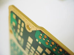
Edge metallization
In order to improve the EMC protection of a circuit board, to create an electrical contact to the housing of the assembly or to meet increased cleanliness requirements, the front sides of the circuit board contour can be metallized.
Milled vias
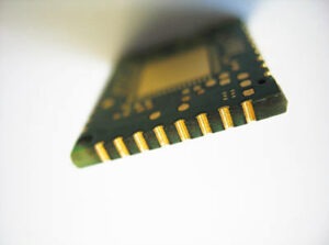
It is possible to produce application-specific components with so-called milled through-holes. The resulting circuit boards can be soldered onto another circuit board as components (interposer) due to their front-side contacting option.
Contour processing
Contour production: milling and scoring
Asymmetrical 1-ply
Asymmetrical 2-ply
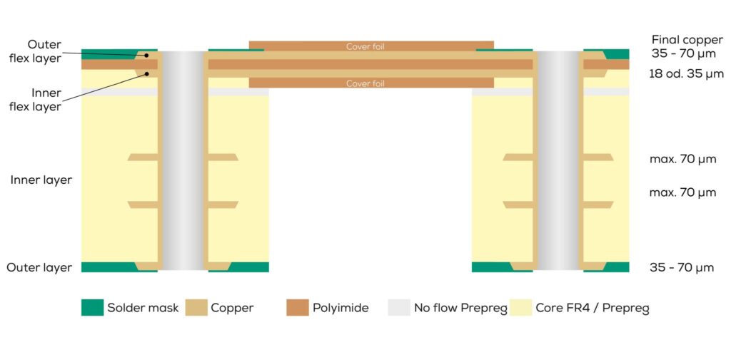
Symmetrical 2-ply
Between 3D integration and cost pressure - expert tips for cost-efficient 3D printed circuit boards
Are you faced with the challenge of assembling your electronics under difficult installation conditions and still have to adhere to tight budgets? Then three-dimensional PCBs could be your key to success. After all, these space-saving wonders are known for increasing packing density, reducing weight and system costs and increasing the reliability of the assembly. Look forward to a new issue of KSG XPERTS, in which Ralph Fiehler and Sebastian Seifert provide you with valuable tips and tricks for cost-efficient 3D PCBs.
In this online seminar


The smart platform for fast and reliable PCB development.
We have bundled all the parameters for you in our Design Compass.
Use the direct line to the experienced PCB experts in our Technical Support department.
We are happy to support you in every phase of your project.

Talk to us in the early development phases of your project and contact our team of experts. Together we will find the solution that will make your product even better.

With a workshop at our premises or at your site, we give you the opportunity to discuss the key technical aspects and features of your project in detail.

From design and layout checks to various calculations and thermal analyses - the experienced, competent Technical Support team will be happy to help you.