Solder resist masks
Additional prints
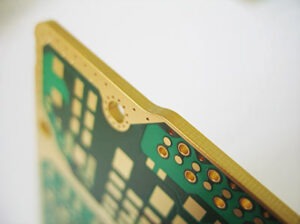
Edge metallization
In order to improve the EMC protection of a circuit board, to create an electrical contact to the housing of the assembly or to meet increased cleanliness requirements, the front sides of the circuit board contour can be metallized.
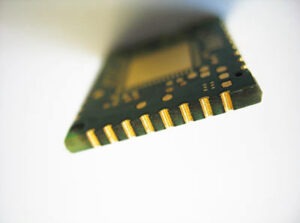
Milled vias
It is possible to produce application-specific components with so-called milled through-holes. The resulting circuit boards can be soldered onto another circuit board as components (interposer) due to their front-side contacting option.
Contour processing
Contour production: milling and scoring
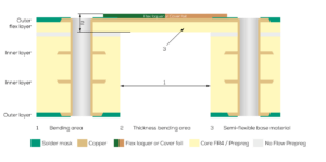
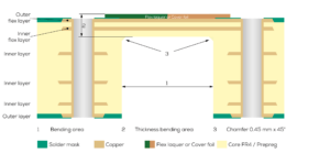
Asymmetrical with a copper layer in the flex area (depth-milled)
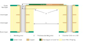
Asymmetrical with two copper layers in the flex area (depth-milled)
Asymmetrical with a copper layer in the flex area (SF technology)